

Micro Vias Be Used in Military Applications
The trend towards miniaturization of electronic products has driven a demand for higher density in printed circuit boards (PCBs). To increase circuitry density while reducing board size, designers use micro vias to reduce the number of holes needed. These are tiny vias with a diameter of 150um or less. They are usually drilled using laser technologies and are extremely precise. Despite their precision, they are known to cause problems during plating and assembly, leading the IPC to issue a warning on their reliability in early 2019.
PCBs have multiple layers sandwiched together to establish the conductive pathway for all components. Traditionally, holes are drilled completely through the layers and then plated with copper to form plated through-holes (PTH). The PTH’s provide the conductive pathways between all of the layers. With the growing popularity of microvias, it is possible to reduce the number of through-holes on a board, which can lower its manufacturing costs and make for a lighter and smaller product.
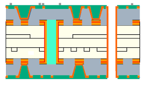
Unlike traditional through-holes, micro vias are blind structures that do not extend to the next layer. They are either buried, or a combination of a blind and buried via, and have a conical frustum shape that slopes inward at the layer transition point to terminate on a pad in the next layer. Microvias can be stacked or staggered, but a staggered design is preferred as a means of improving reliability.
Can Micro Vias Be Used in Military Applications?
Staggered microvias can be used to help improve board performance by moving choke points in the power and ground planes away from overcrowded areas on the board. These choke points can result in localized thermal and electrical hot spots, which in turn can affect board yields. Staggered vias can also be used to move the position of layer transitions for traces or other features that are positioned in overcrowded areas on the PCB.
In general, stacked microvias are less reliable than staggered ones because the voiding associated with them can concentrate stress in the neck region of the via barrel. This makes it more susceptible to fracture during high-temperature cycling, strong vibration or mechanical shock. This can lead to a loss of signal integrity, which is why staggered microvias are preferable in high-reliability applications.
A microvia’s success depends on the etching and plating processes employed, which depend on the laminate materials used and the fabrication method selected. Plasma etching and laser drilling are two popular options for the creation of microvias. Laser drilling offers the advantage of greater positional accuracy, and can even drill into reinforced dielectrics.
In addition, the type of metallization used in a microvia can play a significant role in its reliability. In fact, it is important to work with a qualified PCB fabricator when developing the proposed stackup and selecting the materials used in the final product. They can help ensure that the chosen laminates and drilling methods will be compatible with the manufacturability of microvias. They can also provide advice on which etching and plating processes offer the best fit for your application and manufacturability requirements.