

Steps Involved in RF Circuit Board Design
The primary steps involved in rf circuit board design include designing an RF layout, selecting the correct components, and conducting thorough testing and evaluation. This ensures that the RF circuit boards are ready for manufacturing and can handle the required frequency range. This process may involve a series of iterations to make adjustments and improve performance. RF PCBs are important in the operation of many electronic devices, as they allow for wireless communication and high-speed data processing.
RF circuits require a specific type of PCB to handle high-frequency signals with precision and efficiency. An RF PCB must be able to handle the signal’s transmission speed, amplitude, and phase, as well as provide proper isolation between components. RF PCBs also need to be able to withstand environmental conditions, including temperature extremes.
To achieve this, RF circuits need to be designed with impedance-matched transmission lines, which are designed to reduce signal loss and reflections. These are constructed from a conductor with a characteristic impedance that matches that of the transmission line’s load, and surrounded by a dielectric material.
A good RF PCB design requires careful consideration of the layer stackup and trace lengths, as well as the placement of digital components that interface with RF signals. Typically, the top layer of an RF PCB contains the RF transmission lines and circuits, with the bottom layer providing ground planes, routing for digital signals, and power.
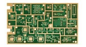
Primary Steps Involved in RF Circuit Board Design
Another important consideration is the choice of materials for the RF circuit board’s layers and bondply. RF circuits require materials with low dissipation factor and dielectric constant to prevent signal degradation due to excessive losses. In addition, the layer thicknesses need to be carefully selected for optimal performance.
Trace lengths must be carefully considered, as RF signals can degrade significantly when they travel over long distances. Additionally, it is vital that RF traces are isolated from other RF traces to prevent cross-talk, which can corrupt the signal’s integrity. Using a single-layer RF PCB can help minimize this issue, as it will increase the amount of separation between traces.
Lastly, RF PCB designs must include appropriate shielding to protect the components and traces from electromagnetic interference (EMI). This includes the use of conductive patterns on the surface of the substrate and incorporating EMI filters and resonant structures to reduce radiated emissions.
Iterative testing and refinement are key to successful RF PCB design. This iterative process often reveals areas where the performance of the RF circuit board can be improved, such as reducing signal loss or mitigating cross-talk. Using simulation software to adjust trace widths, alter the PCB stack-up, and reposition components can help avoid these issues before moving on to the prototype stage. This iterative process can also help identify unforeseen RF-related issues, such as the skin effect, where alternating current tends to flow on the surface of a conductor rather than through it. This can be minimized by implementing a good grounding strategy and stitching vias to provide a continuous return path for current.