

Why is HDI PCB Preferred for Compact Devices?
In today’s fast-paced technological landscape, the demand for smaller, more powerful devices is at an all-time high. As consumer electronics and industrial applications evolve, the need for compact, high-performance circuit boards has become paramount. High-Density Interconnect (HDI) PCBs have emerged as a solution to meet these demands, offering significant advantages in terms of size, functionality, and performance. But why exactly is HDI PCB preferred for compact devices? Let’s delve into the key reasons behind this preference.
1. High Component Density in a Smaller Footprint
One of the standout features of hdi pcb is their ability to achieve a high component density without increasing the overall size of the board. Traditional PCBs, with their relatively larger traces and vias, are limited in terms of the number of components they can accommodate within a given area. In contrast, HDI PCBs utilize finer traces, smaller vias (such as microvias), and multiple layers to create a compact yet highly functional design.
This allows manufacturers to integrate more features and components into the same space, making HDI PCBs ideal for compact devices where space is limited, such as smartphones, wearables, and other portable electronics. By optimizing the PCB layout and routing, HDI technology ensures that devices can offer advanced functionality without compromising on size.
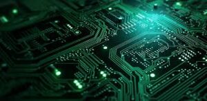
2. Miniaturization of Electronic Devices
Miniaturization is a key trend in electronics, driven by the consumer demand for smaller, lighter devices. From mobile phones to smartwatches, the push for ever-smaller form factors requires an innovative approach to PCB design. HDI PCBs facilitate miniaturization by enabling a higher component density, smaller vias, and thinner traces, all of which contribute to a reduced overall board size.
For example, smartphones and tablets today feature advanced processors, high-resolution screens, and multiple sensors, all packed into slim, lightweight designs. This wouldn’t be possible without HDI PCB technology, which allows designers to fit more components into less space, facilitating the miniaturization of these devices without sacrificing performance.
3. Improved Performance in Smaller Packages
Compact devices often require powerful performance while maintaining a small size. HDI PCBs are a preferred solution for achieving high-speed performance in small form factors. The fine-pitch design of microvias and the ability to use multiple layers in an HDI PCB reduce signal transmission paths and improve signal integrity, which is crucial for high-speed applications.
In compact devices, such as high-performance mobile phones and wearable devices, the reduced distance between components and the efficient routing of signals contribute to faster processing speeds and more reliable connections. This enhanced performance is made possible by the optimized design capabilities of HDI PCBs, which are essential for modern electronics.
4. Thermal Management in Compact Devices
As electronic devices get smaller, managing heat dissipation becomes more challenging. Heat buildup can significantly impact the performance and longevity of components, especially in high-performance, compact devices. HDI PCBs help address this issue by enabling more effective thermal management solutions.
Due to the multi-layer structure and efficient placement of power and ground planes in HDI PCBs, heat is distributed more evenly across the board, helping to keep temperatures in check. Designers can also incorporate features like thermal vias, which direct heat away from heat-sensitive components. This thermal efficiency is critical for compact devices like smartphones, wearables, and IoT devices, where space constraints make traditional cooling solutions less feasible.
5. Higher Reliability and Durability
Compact devices, especially those used in harsh environments (e.g., automotive or medical applications), require reliable and durable circuit boards. HDI PCBs offer superior performance in terms of durability, largely because their design incorporates finer traces, more robust vias, and better overall circuit integrity.
The use of microvias and multiple layers in HDI PCBs also contributes to increased mechanical strength. These design features help minimize the risk of mechanical failure due to shock, vibration, or stress—factors that are particularly important for portable or wearable devices that experience frequent movement or environmental exposure.
Moreover, the improved quality control processes in HDI PCB manufacturing lead to fewer defects and higher reliability. This makes HDI technology an ideal choice for compact devices that need to operate consistently over time, ensuring that users experience minimal downtime or malfunction.
6. Enhanced Electrical Performance
In compact devices, electrical performance is critical, as the compact design often places more demands on the device’s circuitry. HDI PCBs improve electrical performance by reducing signal loss, minimizing electromagnetic interference (EMI), and ensuring better impedance control. The fine-pitch design allows for more precise routing of electrical signals, resulting in faster data transfer and more stable performance.
For example, in applications like high-speed data transmission, wireless communication, and high-frequency devices, HDI PCBs ensure that the electrical signals travel without degradation, enabling the device to operate more efficiently and at higher speeds. This is crucial for compact devices that rely on high-speed communication and processing, such as mobile phones, tablets, and wireless devices.
7. Cost-Effectiveness for Mass Production
While HDI PCBs may involve more advanced manufacturing processes compared to traditional PCBs, they ultimately offer cost benefits, especially when it comes to mass production. Because HDI PCBs are designed for high-density interconnections, manufacturers can produce smaller, more efficient boards, which reduces material costs and allows for the integration of more features within a single PCB.
Furthermore, HDI PCB technology enables the production of smaller and lighter devices, which can lead to savings in packaging, shipping, and assembly costs. For manufacturers of compact consumer electronics, the ability to deliver advanced functionality in a small, cost-effective package is a significant advantage.
Conclusion
HDI PCBs are the ideal choice for compact devices, offering a range of benefits including higher component density, improved performance, thermal management, and enhanced reliability. As the demand for smaller, more powerful devices continues to grow, HDI technology will remain at the forefront of PCB innovation. Whether in smartphones, wearables, or other portable electronics, HDI PCBs play a critical role in helping manufacturers meet the challenges of modern electronics by enabling smaller, faster, and more efficient devices.